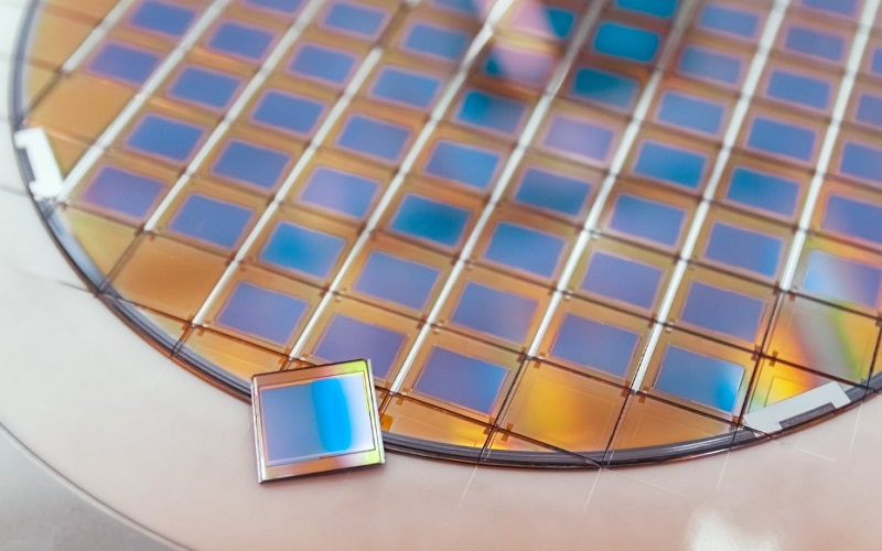
Wafer dicing is a crucial process in the semiconductor and microelectronics industry that involves cutting a semiconductor wafer into individual chips or dice. This comprehensive guide provides an overview of the key aspects of wafer dicing, from its purpose and methods to equipment and quality control measures.
Table of Contents:
-
Introduction to Wafer Dicing
- Definition and Purpose
- Importance in Semiconductor Manufacturing
-
Materials Used in Wafer Dicing
- Silicon Wafers
- Other Substrates (e.g., ceramics, glass)
-
Methods of Wafer Dicing
- Blade Dicing
- Laser Dicing
- Comparison of Methods
-
Key Considerations for Blade Dicing
- Blade Types and Characteristics
- Dicing Parameters (e.g., feed rate, blade speed)
- Blade Maintenance
-
Key Considerations for Laser Dicing
- Laser Types (e.g., UV, IR)
- Laser Ablation Process
- Precision and Material Compatibility
-
Quality Control in Wafer Dicing
- Inspection and Metrology
- Tolerances and Specifications
- Detection and Prevention of Defects
-
Equipment Used in Wafer Dicing
- Dicing Saws
- Laser Dicing Machines
- Cleanroom Facilities
-
Wafer Preparation for Dicing
- Wafer Cleaning
- Scribing Process
- Inspection and Defect Mapping
-
Dicing Process Workflow
- Alignment and Positioning
- Dicing Operation
- Die Separation
- Post-Dicing Inspection
-
Common Defects in Wafer Dicing
- Chipping and Fracture
- Cracks and Cleaving
- Die Misalignment
- Blade Issues
- Delamination
- Burrs
- Contamination
-
Applications of Diced Wafers
- Microelectronics and Semiconductors
- MEMS (Micro-Electro-Mechanical Systems)
- Photonics and Optoelectronics
- Sensor Technology
- Medical Devices
- Aerospace and Defense
-
Advancements and Trends in Wafer Dicing
- Advanced Materials
- Miniaturization and 3D Packaging
- Industry 4.0 and Automation
- Environmental Considerations
-
Choosing a Wafer Dicing Manufacturer
- Evaluation Criteria
- Quality Assurance and Certifications
- Geographic Considerations
- Communication and Collaboration
-
Conclusion
- Recap of Key Points
- Importance of Wafer Dicing in Modern Electronics
This ultimate guide provides a comprehensive overview of wafer dicing, from its fundamental principles to practical considerations and industry trends. Whether you are involved in semiconductor manufacturing or the development of advanced electronic devices, this guide will help you understand the intricacies of wafer dicing and make informed decisions in your projects.